junction transistor - translation to russian
Diclib.com
ChatGPT AI Dictionary
Enter a word or phrase in any language 👆
Language:     

Translation and analysis of words by ChatGPT artificial intelligence

On this page you can get a detailed analysis of a word or phrase, produced by the best artificial intelligence technology to date:

  • how the word is used
  • frequency of use
  • it is used more often in oral or written speech
  • word translation options
  • usage examples (several phrases with translation)
  • etymology

junction transistor - translation to russian

TRANSISTOR THAT USES BOTH ELECTRONS AND HOLES AS CHARGE CARRIERS
BJT; P-n-p transistor; N-p-n transistor; Bjt; Bipolar junction transistors; Bipolar Junction Transistor; Collector current; Bjt transistor; Emitter, base, and collector; Ebers-Moll; PNP (transistor polarity); Ebers-Moll model; PNP transistor; NPN transistor; Transistor beta; Ebers–Moll model; Bipolar transistor; Bipolar transistors; Power BJT; Junction transistor; P–n–p transistor; N–p–n transistor; H-parameter model; Emitter, base and collector; Emitter current; VBIC
  • Approximated Ebers&ndash;Moll model for an NPN transistor in the forward active mode. The collector diode is reverse-biased so ''I''<sub>CD</sub> is virtually zero. Most of the emitter diode current (''α''<sub>F</sub> is nearly 1) is drawn from the collector, providing the amplification of the base current.
  • Generalized h-parameter model of an NPN BJT.<br />''Replace '''x''' with '''e''', '''b''' or '''c''' for CE, CB and CC topologies respectively.''
  • 3D model of bipolar transistor
  • Symbol for NPN bipolar transistor with current flow direction
  • depleted regions]].
  •  url=https://archive.org/details/microelectronicc0000sedr/page/903
 }}</ref> ''I''<sub>B</sub>, ''I''<sub>C</sub> and ''I''<sub>E</sub> are the base, collector and emitter currents; ''I''<sub>CD</sub> and ''I''<sub>ED</sub> are the collector and emitter diode currents; ''α''<sub>F</sub> and ''α''<sub>R</sub> are the forward and reverse common-base current gains.
  • Ebers&ndash;Moll model for a PNP transistor
  • Hybrid-pi model
  • Simplified cross section of a planar ''NPN'' bipolar junction transistor
  • Structure and use of NPN transistor. Arrow according to schematic.
  • [[Band diagram]] for NPN transistor in active mode, showing injection of electrons from emitter to base, and their overshoot into the collector
  • [[Band diagram]] for NPN transistor at equilibrium

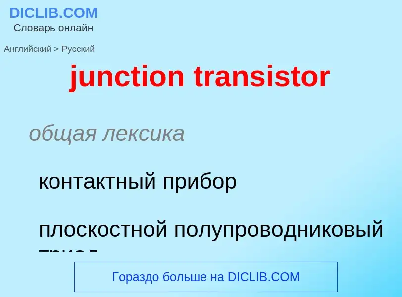
junction transistor         

общая лексика

контактный прибор

плоскостной полупроводниковый триод

плоскостной транзистор

bipolar transistor         

полупроводники

биполярный транзистор

grown-junction transistor         
  • An NPN grown-junction transistor with the cover removed to show the germanium ingot and the base wire.
FIRST TYPE OF BIPOLAR JUNCTION TRANSISTOR MADE
Grown junction transistor

общая лексика

тянутый плоскостной полупроводниковый триод

Definition

bipolar transistor
<electronics> A transistor made from a sandwich of n- and p-type semiconductor material: either npn or pnp. The middle section is known as the "base" and the other two as the "collector" and "emitter". When used as an amplifying element, the base to emitter junction is in a "forward-biased" (conducting) condition, and the base to collector junction is "reverse-biased" or non-conducting. Small changes in the base to emitter current (the input signal) cause either holes (for pnp devices) or free electrons (for npn) to enter the base from the emitter. The attracting voltage of the collector causes the majority of these charges to cross into and be collected by the collector, resulting in amplification. Contrast field effect transistor. (1995-10-04)

Wikipedia

Bipolar junction transistor

A bipolar junction transistor (BJT) is a type of transistor that uses both electrons and electron holes as charge carriers. In contrast, a unipolar transistor, such as a field-effect transistor, uses only one kind of charge carrier. A bipolar transistor allows a small current injected at one of its terminals to control a much larger current flowing between the terminals, making the device capable of amplification or switching.

BJTs use two p–n junctions between two semiconductor types, n-type and p-type, which are regions in a single crystal of material. The junctions can be made in several different ways, such as changing the doping of the semiconductor material as it is grown, by depositing metal pellets to form alloy junctions, or by such methods as diffusion of n-type and p-type doping substances into the crystal. The superior predictability and performance of junction transistors quickly displaced the original point-contact transistor. Diffused transistors, along with other components, are elements of integrated circuits for analog and digital functions. Hundreds of bipolar junction transistors can be made in one circuit at very low cost.

Bipolar transistor integrated circuits were the main active devices of a generation of mainframe and minicomputers, but most computer systems now use CMOS integrated circuits relying on field-effect transistors. Bipolar transistors are still used for amplification of signals, switching, and in mixed-signal integrated circuits using BiCMOS. Specialized types are used for high voltage switches, for radio-frequency amplifiers, or for switching high currents.
What is the Russian for junction transistor? Translation of &#39junction transistor&#39 to Russian